Whatsapp
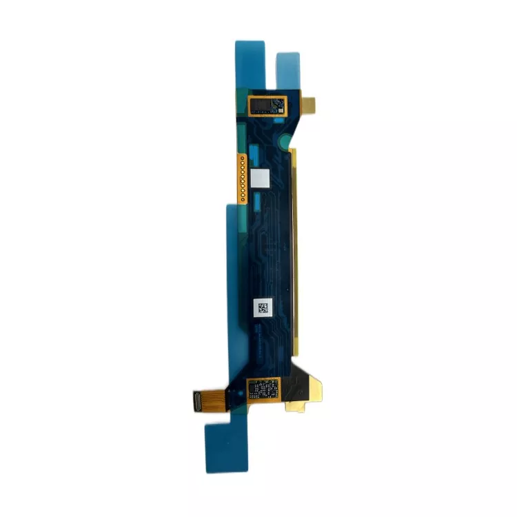
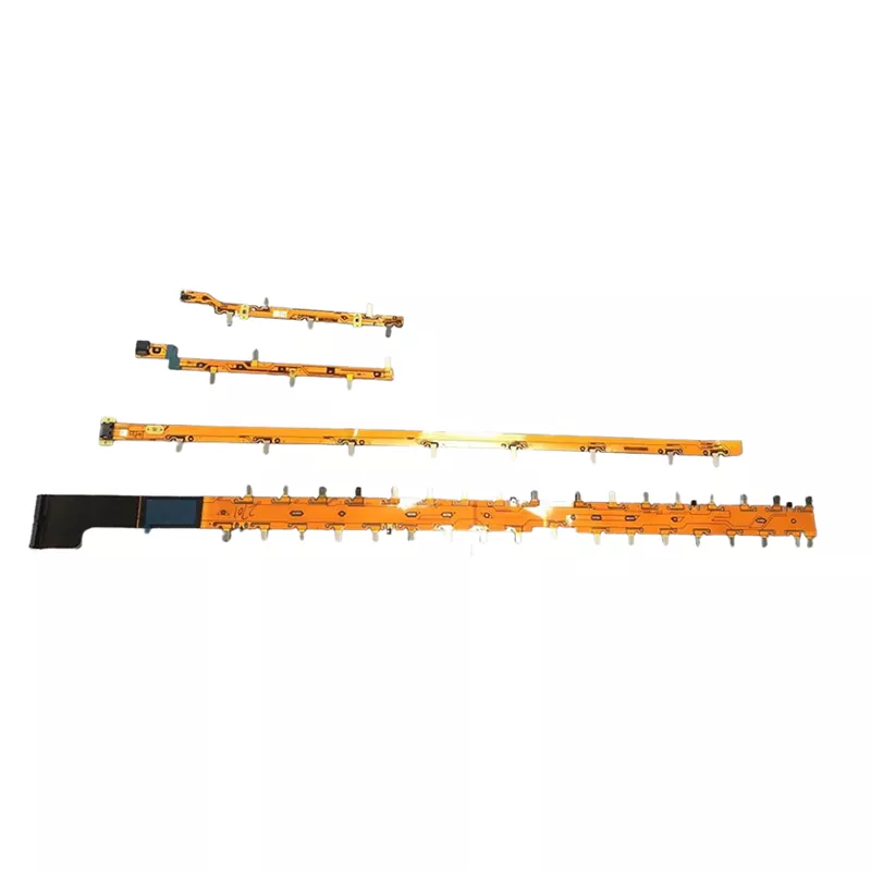
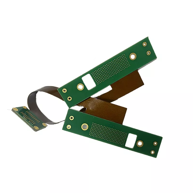
Flexible printed circuit boards (FPCs) are an indispensable component of modern electronic devices, ubiquitous from foldable smartphone screens to precision probes in medical devices. Flash plating is a core manufacturing process that enables high performance and high reliability in FPCs.
Process Overview: The Complete Journey from Drilling to Copper Plating
The flash plating process in FPC manufacturing is a series of precise operations. The entire process begins with drilling, creating pathways for circuit connections on the flexible substrate. Next comes the copper plating process, where a thin layer of copper is chemically deposited on the hole walls, establishing a conductive foundation for subsequent electroplating.
The core of the flash plating process lies in the word "flash," requiring a critical plating layer to be completed within just 3 minutes. This thin and uniform copper layer is the foundation for subsequent processing. Afterward, the dry film lamination stage begins, covering the board surface with a photosensitive film to prepare for the formation of the circuit pattern.
The exposure and development stages determine the precise shape of the circuit. Through light and chemical treatment, unwanted dry film is removed, exposing the areas requiring secondary copper plating. The final secondary copper plating thickens the circuit to the required functional thickness, ensuring stable and reliable current transmission.
Each step is like a meticulously choreographed dance; even a slight deviation can lead to functional defects in the entire circuit board. This requirement for precision is why FPC manufacturing is known as the "precision art of the electronics industry."
Key Technology: Special Treatment of Bending Areas
In FPC manufacturing, handling bending areas is one of the most challenging aspects. To ensure the reliability of the circuit board during repeated bending, copper plating is not allowed in the bending areas. This is one of the fundamental differences between FPC and rigid PCB manufacturing.
The bending area is the "joint" of the FPC. If this area were also copper-plated, the increased copper foil thickness would reduce the material's flexibility. Over time, repeated bending will cause fatigue cracking of the copper layer, severely affecting the product's lifespan.
In actual production, the unplated bending areas are slightly larger than the pure adhesive openings. This is to prevent copper plating solution from penetrating into the bending areas. This "reserved space" design ensures that circuit functionality is not affected while maximizing the protection of the bending area's flexibility.
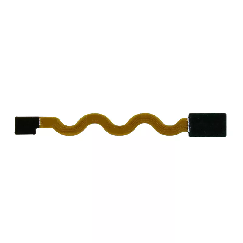
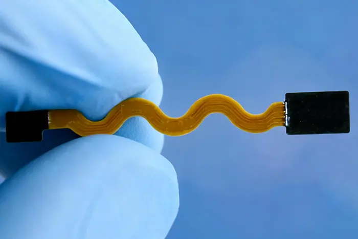
The treatment of the joints is equally crucial. Manufacturing specifications explicitly require that joints not be located in delamination areas and must employ a wavy design. This design effectively disperses stress, preventing joint breakage caused by stress concentration.
Imagine a smartphone's foldable screen, subjected to dozens, even hundreds, of bends daily. It is the perfect execution of these process details that ensures the device will not fail due to FPC malfunctions during long-term use.
Precise Control: Dual Requirements of Time and Area The word "flash" in the name of the flash plating process reflects the speed requirement of this step. Industry standards clearly stipulate that flash plating must be completed within 3 minutes. This is not an arbitrary time setting, but rather the optimal solution derived from extensive experimentation and actual production experience.
Too short a time results in insufficient copper deposition, failing to provide a sufficient conductive base for subsequent processes; too long a time may lead to uneven copper layers, resulting in coarse grains and insufficient adhesion. The 3-minute time window achieves a perfect balance between efficiency and quality.
The secondary copper plating stage has a different focus. Here, the copper plating area must be precisely specified. This requirement, seemingly simple, actually relates to multiple aspects such as product quality control, cost management, and traceability.
The copper plating area directly affects the resistance and current-carrying capacity of the final product. Precise control of the area means precise control of circuit performance, which is one of the key differences between high-end FPCs and ordinary products.
From a cost perspective, copper is one of the main material costs in FPC manufacturing. Precise control of the copper plating area can avoid unnecessary material waste, which can bring significant cost savings in mass production. More importantly, area data provides a basis for quality tracking; once a product problem occurs, it can be quickly traced back to specific process parameters.
Quality Assurance: Multi-layered Control Ensures Zero Defects
The reliability of FPCs begins with every detail of the process design. In addition to special treatment of bending areas and joints, multiple layers of quality control measures are implemented throughout the entire process.
In the dry film lamination stage after flash plating, the uniformity of film thickness directly affects the exposure and development effects. Modern production lines are usually equipped with online monitoring systems to measure film thickness in real time and automatically adjust process parameters to ensure consistency.
The precision of the exposure stage determines the clarity of the circuit pattern. Advanced exposure machines utilize direct laser imaging technology, enabling the production of linewidths and spacings smaller than 10 micrometers, meeting the design requirements of today's high-density FPCs.
Quality control in the secondary copper plating stage is particularly critical. Besides area control, copper layer thickness, uniformity, and crystal structure all require strict monitoring. Modern electroplating lines are typically equipped with X-ray thickness gauges and electrochemical analyzers to monitor plating quality in real time.
These multi-layered quality control measures ensure that the final product meets the stringent requirements of various fields, from consumer electronics to automotive electronics and medical devices. In automotive applications, FPCs may need to withstand temperature variations from -40°C to 125°C; in medical devices, long-term stability and biocompatibility must be guaranteed.
The flash plating process is like the art of "drawing" circuits on a flexible substrate; each step embodies engineers' pursuit of a balance between precision and flexibility. With the rise of wearable devices, flexible displays, and micro-medical devices, FPC manufacturing processes will continue to evolve towards greater precision, flexibility, and reliability, becoming an invisible link connecting the future electronic world.